
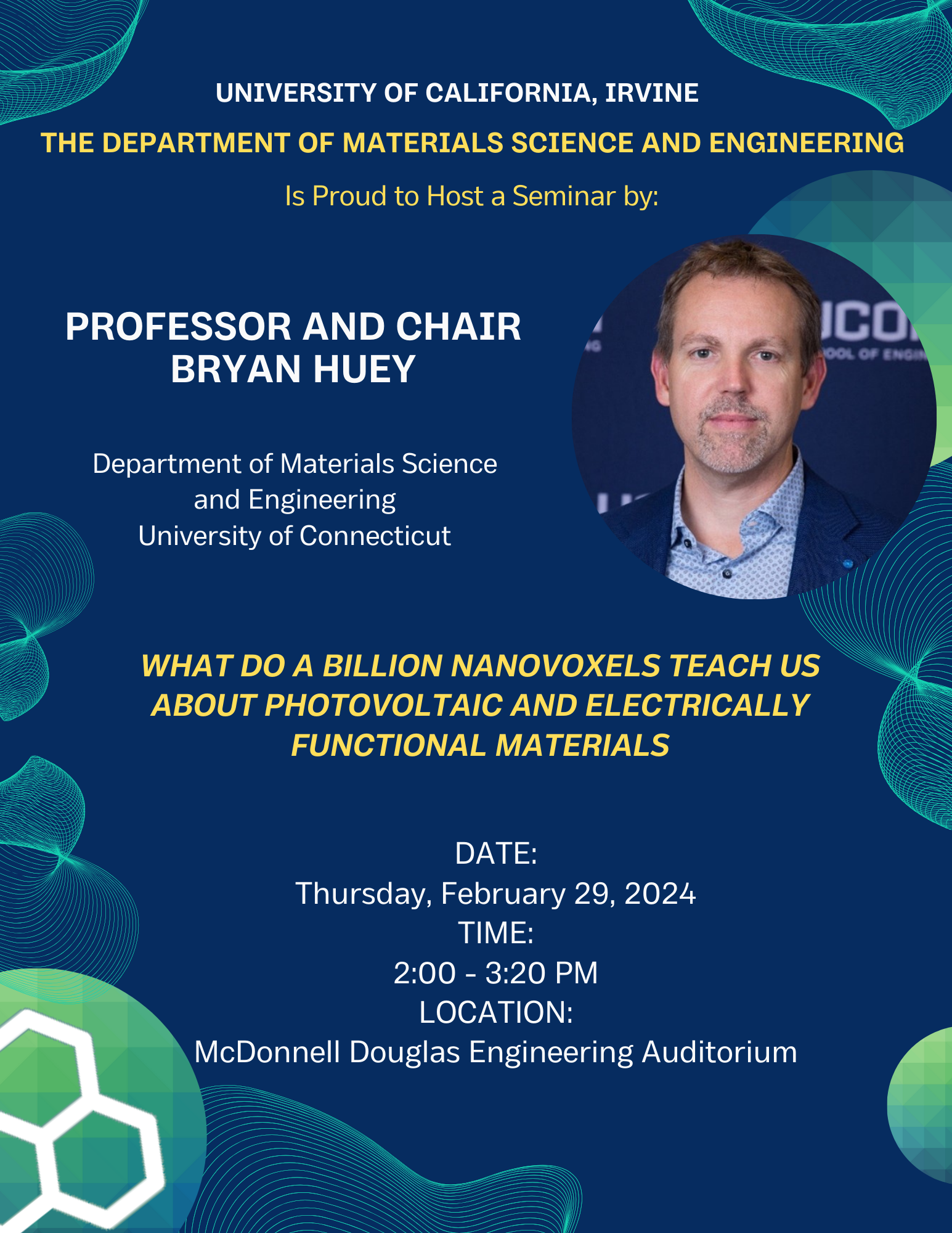
MSE 298 Seminar: What Do A Billion Nanovoxels Teach Us About Photovoltaic and Electrically Functional Materials
Professor and Chair
Department of Materials Science and Engineering
University of Connecticut
Abstract: Nano- and meso- scale materials properties are crucial to the macroscopic performance of a wide range of modern devices. Particularly for photoconductors, piezoelectrics and dielectrics, investigations with Atomic Force Microscopy are especially insightful for elucidating the influence of grain boundaries, orientation, strain, microstructural defects and/or engineered heterogeneities. However, practical devices are often sensitive to, or even controlled by, three-dimensional effects such as patterning, sub-surface effects, or thickness dependencies, all of which can be further sensitive to microstructure, concentration, field gradients, etc. Accordingly, we have developed a serial sectioning approach to achieve “Tomographic AFM” for volumetric materials property mapping. Voxels are finerthan 10 nm3, capable of distinguishing super lattice layers as fine as 16 unit cells thick. With polycrystalline photovoltaics such CdTe or MAPbI3, T-AFM literally uncovers new pathways to improve carrier separation via inter- and intra- granular defects (Luria, Nature Energy, 2017; Song, Nature Communications, 2020). ForBiFeO3, Tomographic AFM confirms Kay-Dunn thickness scaling for ferroelectricity (Steffes, PNAS, 2018), and even co-located domain and current maps which together reveal sub-surface topological defects. Direct effects of lateral strain are resolved for nanostructured composites (Song, Advanced Functional Materials, 2021). Analyses of boundary curvature (ErMnO3) and ultra thin films (Bi5FeTi3O15), as wellas ultra-resolution surface lithography, will also be discussed. Such nano-volumetric insight and control is increasingly important for engineering optimal performance and reliability of real-world, three-dimensional materials devices.
Bio: Professor Bryan Huey has been the department head for MSE at UConn since 2018. He is an expert in the development and application of advanced variations of Atomic Force Microscopy for studying piezoelectrics, multiferroics, photovoltaics, MEMS and biological cells and tissue. This includes simultaneous AFM and three-Dfluorescence, high speed AFM and a recent focus advancing Tomographic AFM. He is the immediate past chair for the nationwide association of MSE department heads (UMC), previously chaired the 1200 person Basic Science Division of the American Ceramic Society, was one of five overall organizers for the 7000 attendee 2019 MRS Fall Meeting and co-organized previous EMA and US-Japan Dielectrics conferences.
www.hueyafmlabs.mse.uconn.edu
Share
Related Content
| Attachment | Size |
|---|---|
| 1.11 MB | |
| 698.24 KB |
Upcoming Events
-
EECS Seminar: Less Compute, More Intelligence – Efficient and Autonomous Generative AI and Agents
-
MAE 298: Microscopic Robots that Sense, Act and Compute
-
CBE 298 Seminar: Interface Modification for Electrocatalysis
-
CEE Ph.D. Defense Announcement: Machine Learning and Remote Sensing for Environmental Modeling - From Large-Scale Streamflow Forecasting to Malaria Risk Mapping
-
CBE Special Seminar: Operando Electrochemical Methods at Dynamic Energy Materials Interfaces