ChEMS Seminar: Linking Nanoscopic and Macroscopic Conductivity in Polycrystalline Ceramics using Advanced Transmission Electron Microscopy

Laboratory for Electrochemical Interfaces
Department of Nuclear Science and Engineering
Massachusetts Institute of Technology, Cambridge, MA
Abstract: The properties and behavior of polycrystalline materials in service and during processing are influenced strongly by grain boundaries. Understanding the chemical and charge transport properties of grain boundaries in non-stoichiometric oxides is critical for developing ion-conducting solids for catalysis, sensing, energy conversion and storage, information storage and elsewhere. However, despite their wide-ranging scientific and technical relevance, grain boundary characterization, elucidation and optimization is hindered by significant fluctuation in atomic structure, composition and chemistry within nanometers or Ångstroms of the boundary interface. Hence, a need exists to develop and apply multiscale correlated experimental methods that probe grain boundary properties over the many relevant length scales.
I will discuss correlated multiscale transmission electron microscopy methods and electrochemical transport measurements used to illustrate the impact of nanoscale grain boundary properties on the macroscopic electrical conductivity of CeO2-based polycrystalline ceramics. In this work, local composition and electronic structure measured using aberration-corrected and monochromated electron probes provides unique insights into the origin of charge transport processes at grain boundaries. Additionally, I will present a novel electron microscopy approach to show a critical relationship between the relative misorientation of adjacent grains and the grain boundary composition. This is the basis for a new framework to determine the grain boundary conductivity distribution, which describes the boundary-to-boundary variation in ionic conductivity within a polycrystalline oxygen ion conductor. This seminar aims to provide new insights into fundamental interface and grain boundary science of non-stoichiometric oxide ceramics, and to highlight how nanoscale material properties may be manipulated to control macroscale charge transport in oxide electrical ceramics.
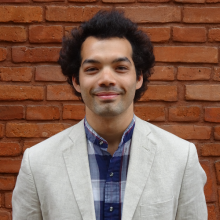
Bio: Bowman is a postdoctoral associate at MIT working in the Laboratory for Electrochemical Interfaces with Professor Bilge Yildiz as part of the MIT Energy Initiative. He completed a doctorate in materials science and engineering with Professor Peter Crozier at Arizona State University (2016), during which time he also was a visiting scholar in the Electrochemical Materials Group of Professor Jennifer L.M. Rupp at ETH Zurich in Switzerland. His current research focuses on developing nanoengineered oxide coatings to mitigate hydrogen embrittlement of metals used in nuclear reactors, geothermal systems and infrastructure for a hydrogen economy. Previously, he applied advanced transmission electron microscopy to the study of chemical and electrical properties of grain boundaries and interfaces in electroceramic oxides. He also is the founder and current program chair of the pre-meeting congress for students, postdocs and early-career professionals in microscopy and microanalysis, which is held annually ahead of the Microscopy and Microanalysis (M&M) Meeting.
Host: Martha Mecartney
Share
Upcoming Events
-
EECS Seminar: Steering Diffusion Models for Generative AI, From Multimodal Priors to Test-Time Scaling
-
MAE 298 SEMINAR: Hypersonic Viscous Aerothermochemistry - External Aerothermodynamics and Scramjet Fuel-Air Mixing
-
CBE 298 Seminar: Finding Catalysts of Gut Reactions - The Gut Microbiota in Disease Onset and Treatment
-
CEE Seminar: Confirming a Critical Foundation of Global Warming - Direct Observational Evidence from Space of the Impact of CO2 Growth on Infrared Spectra
-
CBE 298 Seminar: Teaching Transport Phenomena Through Observation - From Einstein’s Tea Leaves to Dissolving Skittles
