
Tackling the Challenge of Prolonging Battery Life in Cell Phones, Laptops with Advanced Radio-Frequency Technology
July 18, 2006 - Imagine charging a cell phone just once a week, or a personal laptop once a month, forgoing large battery packs and cords, and always having to locate an inconvenient electrical outlet. Engineers at the
Supported by a $200,000 grant from the Industry-University Cooperative Research Program (IUCRP), Payam Heydari, assistant professor of electrical engineering and computer science, is exploring new advanced power optimization techniques for ultra-low power (ULP) RF integrated circuit designs, developing sub-mW radios that operate at an RF frequency of 1 GHz within a wireless receiver.
Prototype 1 GHz low-noise amplifier (LNA) circuits were produced using a Complementary Metal Oxide Semiconductor (CMOS) 180 nm process, together with two additional LNA circuits, which were created and tested in the same process for comparison. These LNA circuits included a ULP common-gate LNA at 1057 µm x 865 µm, and a ULP LNA with inductive feedback at 1050 µm x 865 µm.
Measurement results displayed a power consumption of only 100 µW, functioning 10 times better than current RF technologies at 1 mW, while still maintaining their overall quality. The device is the first high-performance RF LNA circuit fabricated in CMOS to operate at this power level.
“Power minimization is crucial in emerging technologies, such as high performance cell phones, laptops, PDAs, and other wireless communication tools used daily by consumers, in order for the device to reach its maximum potential for the longest time possible,” Heydari said.
CMOS technologies are prime candidates for the future developments of ULP integrated circuits because of their high integration capability and continual scaled feature size. For example, the same LNA fabricated in a 130 nm process consumes just 75 µW of power.
“These results demonstrate that the proposed ultra-low-power LNAs exhibit higher gain, lower noise-figure, and better linearity while consuming far less power compared to prior work. Essentially, future wireless products that use these radios can save a significant amount of battery power, without compromising their performance,” explained Heydari.
He expects that these low-power RF integrated circuits (IC) will become commercially available within the next five years. His team is now working on the integration of the entire silicon-based transceiver, as well as the chip packaging design process in partnership with MOSIS, a production service company that targets ICs and related products.
Heydari’s research was presented at the 2006
Research Images:
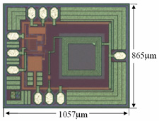
Common-gate LNA fabricated in CMOS 180nm process
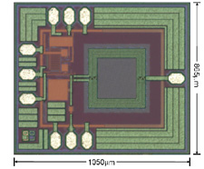
ULP LNA with inductive feedback fabricated in CMOS 180nm process
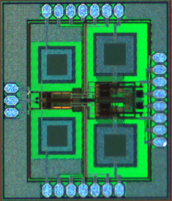
Whole ULP radio fabricated in CMOS 180nm process